logo logologo

Language
Search...

Products

Products

Home > Products > Holtek MCUs > 8-bit(Flash)MCU

Holtek MCU HT67F40-HT67F50

The HT67FXX series of devices are Flash Memory A/D with LCD type 8-bit high performance RISC architecture microcontrollers, designed for applications that interface directly to analog signals and which require an LCD interface.

General Description

The HT67FXX series of devices are Flash Memory A/D with LCD type 8-bit high performance  RISC architecture microcontrollers, designed for applications that interface directly to analog signals  and which require an LCD interface. Offering users the convenience of Flash Memory multi-programming features, these devices also include a wide range of functions and features. Other  memory includes an area of RAM Data Memory as well as an area of EEPROM memory for storage  of non-volatile data such as serial numbers, calibration data etc.

Analog features include a multi-channel 12-bit A/D converter and dual comparator functions.  Multiple and extremely flexible Timer Modules provide timing, pulse generation and PWM  generation functions. Communication with the outside world is catered for by including fully  integrated SPI or I2 C interface functions, two popular interfaces which provide designers with a  means of easy communication with external peripheral hardware. Protective features such as an  internal Watchdog Timer, Low Voltage Reset and Low Voltage Detector coupled with excellent noise  immunity and ESD protection ensure that reliable operation is maintained in hostile electrical  environments.

A full choice of HXT, LXT, ERC, HIRC and LIRC oscillator functions are provided including a  fully integrated system oscillator which requires no external components for its implementation. The  ability to operate and switch dynamically between a range of operating modes using different clock  sources gives users the ability to optimise microcontroller operation and minimise power  consumption.

The inclusion of flexible I/O programming features, Time-Base functions along with many other  features ensure that the devices will find excellent use in applications such as electronic metering,  environmental monitoring, handheld instruments, household appliances, electronically controlled  tools, motor driving in addition to many others.

Product Features

  • CPU Features

    • Operating voltage

    ♦ fSYS= 4MHz: 2.2V~5.5V

    ♦ fSYS= 8MHz: 2.4V~5.5V

    ♦ fSYS= 12MHz: 2.7V~5.5V

    ♦ fSYS= 16MHz: 4.5V~5.5V

    • Up to 0.25us instruction cycle with 16MHz system clock at VDD=5V

    • Power down and wake-up functions to reduce power consumption

    • Six oscillators

    ♦ External Crystal - HXT

    ♦ External 32.768kHz Crystal - LXT

    ♦ External RC - ERC

    ♦ External Clock - EC

    ♦ Internal RC - HIRC

    ♦ Internal 32kHz RC - LIRC

    • Multi-mode operation: NORMAL, SLOW, IDLE and SLEEP

    • Fully integrated internal 4MHz, 8MHz and 12MHz oscillator requires no external components

    • All instructions executed in one or two instruction cycles

    • Table read instructions

    • 61 powerful instructions

    • Up to 12-level subroutine nesting

    • Bit manipulation instruction

  • Peripheral Features

    • Flash Program Memory: 2Kx15 ~ 12Kx16

    • RAM Data Memory: 128x8 ~ 640x8

    • EEPROM Memory: 64x8 ~ 256x8

    • Watchdog Timer function

    • Up to 64 bidirectional I/O lines

    • LCD driver function

    • Multiple pin-shared external interrupts

    • Multiple Timer Module for time measure, input capture, compare match output, PWM output or  single pulse output function

    • Serial Interfaces Module with Dual SPI and I2 C interfaces

    • Single Serial SPI Interface

    • Dual Comparator functions

    • Dual Time-Base functions for generation of fixed time interrupt signals

    • Multi-channel 12-bit resolution A/D converter

    • Low voltage reset function

    • Low voltage detect function

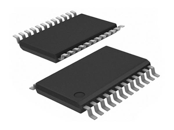
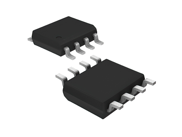
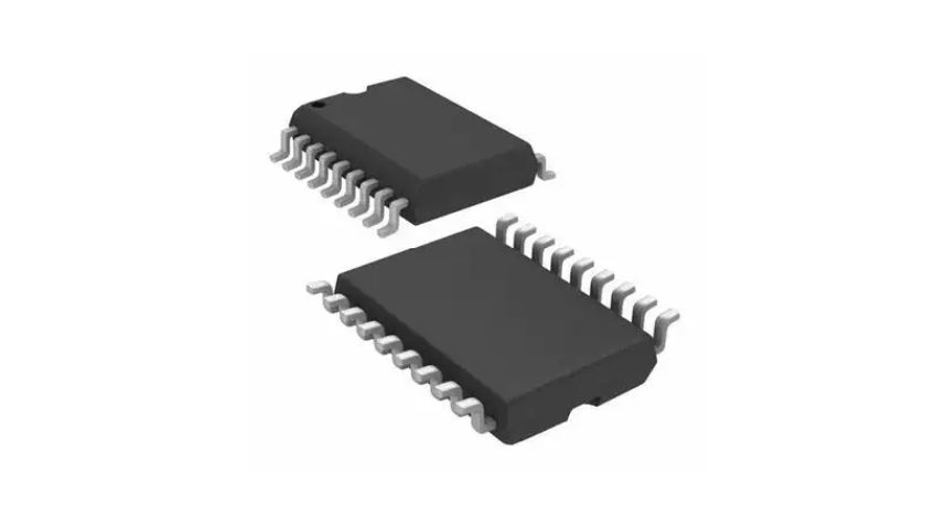
    • Wide range of available package types

    • Flash program memory can be re-programmed up to 10,000 times

    • Flash program memory data retention > 10 years

    • EEPROM data memory can be re-programmed up to 100,000 times

    • EEPROM data memory data retention > 10 years

Block Diagram

Holtek MCU HT68F0017


Pin Assignment

Holtek MCU HT68F0017


Pin Description

Holtek MCU HT68F0017


How to Order

You can get your Holtek MCU HT67F40-HT67F50 solution by flling out the form below and we will contact you immediately.

Want to turn your idea into reality? Contact YFM Support
Copyright © 2022 Shenzhen Yufan Microelectronics Co., Ltd. All Rights Reserved. | Sitemap

Contact

Copyright © 2022 Shenzhen Yufan Microelectronics Co., Ltd. All Rights Reserved. | { fanyi('Sitemap') }}
Online

Email

Message
TOP