Search...


The HOLTEK HT32F52220/52230 devices are high performance, low power consumption 32-bit microcontrollers based around an Arm® Cortex®-M0+ processor core. The Cortex®-M0+ is a next-generation processor core which is tightly coupled with Nested Vectored Interrupt Controller (NVIC), SysTick timer, and including advanced debug support.The devices operate at a frequency of up to 40 MHz for HT32F52220/52230 with a Flash accelerator to obtain maximum efficiency. It provides up to 32 KB of embedded Flash memory for code/data storage and 4 KB of embedded SRAM memory for system operation and application program usage. A variety of peripherals, such as ADC, I2C, USART, UART, SPI, GPTM, SCTM, BFTM, WDT, SW-DP (Serial Wire Debug Port), etc., are also implemented in the device series. Several power saving modes provide the flexibility for maximum optimization between wakeup latency and power consumption, an especially important consideration in low power applications.The above features ensure that the devices are suitable for use in a wide range of applications, especially in areas such as white goods application control, power monitors, alarm systems, consumer products, handheld equipment, data logging applications, motor control and so on.
The devices operate at a frequency of up to 40 MHz for HT32F52230/52230 with a Flash accelerator to obtain maximum efficiency. It provides up to 32 KB of embedded Flash memory for code/data storage and 4 KB of embedded SRAM memory for system operation and application program usage. A variety of peripherals, such as ADC, I 2 C, USART, UART, SPI, GPTM, SCTM, BFTM, WDT, SW-DP (Serial Wire Debug Port), etc., are also implemented in the device series. Several power saving modes provide the flexibility for maximum optimization between wakeup latency and power consumption, an especially important consideration in low power applications.
The above features ensure that the devices are suitable for use in a wide range of applications, especially in areas such as white goods application control, power monitors, alarm systems, consumer products, handheld equipment, data logging applications, motor control and so on.
32-bit Arm ® Cortex ® -M0+ processor core.
Up to 40 MHz operating frequency.
0.93 DMIPS/MHz (Dhrystone v2.1).
Single-cycle multiplication.
Integrated Nested Vectored Interrupt Controller (NVIC).
24-bit SysTick timer.
The Cortex ® -M0+ processor is a very low gate count, highly energy efficient processor that is intended for microcontroller and deeply embedded applications that require an area optimized, low-power processor. The processor is based on the ARMv6-M architecture and supports Thumb ® instruction sets; single-cycle I/O port; hardware multiplier and low latency interrupt respond time.
4 KB on-chip SRAM.
Supports multiple boot modes.
The Arm ® Cortex ® -M0+ processor accesses and debug accesses share the single external interface to external AHB peripherals. The processor accesses take priority over debug accesses. The maximum address range of the Cortex ® -M0+ is 4 GB since it has a 32-bit bus address width. Additionally, a pre-defined memory map is provided by the Cortex ® -M0+ processor to reduce the software complexity of repeated implementation by different device vendors. However, some regions are used by the Arm ® Cortex ® -M0+ system peripherals. Refer to the Arm ® Cortex ® -M0+ Technical Reference Manual for more information. Figure 2 shows the memory map of the HT32F522320/52230 series of devices, including code, SRAM, peripheral, and other pre-defined regions.
Flash accelerator for maximum efficiency.
32-bit word programming with In System Programming Interface (ISP) and In ApplicationProgramming (IAP).
Flash protection capability to prevent illegal access.
The Flash Memory Controller, FMC, provides all the necessary functions and pre-fetch buffer for the embedded on-chip Flash Memory. Since the access speed of the Flash Memory is slower than the CPU, a wide access interface with a pre-fetch buffer and cache are provided for the Flash Memory in order to reduce the CPU waiting time which will cause CPU instruction execution delays. Flash Memory word program/page erase functions are also provided.
Supply supervisor: Power On Reset / Power Down Reset – POR/PDR; Brown-out Detector BOD;Programmable Low Voltage Detector – LVD.
The Reset Control Unit, RSTCU, has three kinds of reset, a power on reset, a system reset and an APB unit reset. The power on reset, known as a cold reset, resets the full system during power up. A system reset resets the processor core and peripheral IP components with the exception of the SW-DP controller. The resets can be triggered by an external signal, internal events and the reset generators.
External 4 to 16 MHz crystal oscillator.
Internal 8 MHz RC oscillator trimmed to ±2 % accuracy at 3.3V operating voltage and 25°C operating temperature.
Internal 32 kHz RC oscillator.
Integrated system clock PLL.
Independent clock divider and gating bits for peripheral clock sources.
The Clock Control unit, CKCU, provides a range of oscillator and clock functions. These include a High Speed Internal RC oscillator (HSI), a High Speed External crystal oscillator (HSE), a Low Speed Internal RC oscillator (LSI), a Phase Lock Loop (PLL), a HSE clock monitor, clock prescalers, clock multiplexers, APB clock divider and gating circuitry. The AHB, APB and Cortex ® -M0+ clocks are derived from the system clock (CK_SYS) which can come from the HSI, HSE or PLL. The Watchdog Timer and Real Time Clock (RTC) use the LSI as their clock source.
Single V DD power supply: 2.0 V to 3.6 V.
Integrated 1.5 V LDO regulator for CPU core, peripherals and memories power supply.
Two power domains: V DD , 1.5 V.
Four power saving modes.
Sleep, Deep-Sleep1, Deep-Sleep2, Power-Down:Power consumption can be regarded as one of the most important issues for many embedded system applications. Accordingly the Power Control Unit, PWRCU, in these devices provides many types of power saving modes such as Sleep, Deep-Sleep1, Deep-Sleep2 and Power-Down mode. These operating modes reduce the power consumption and allow the application to achieve the best trade-off between the conflicting demands of CPU operating time, speed and power consumption.
Up to 16 EXTI lines with configurable trigger source and type.
All GPIO pins can be selected as EXTI trigger source.
Source trigger type includes high level, low level, negative edge, positive edge, or both edge.
Individual interrupt enable, wakeup enable and status bits for each EXTI line.
Software interrupt trigger mode for each EXTI line.
Integrated deglitch filter for short pulse blocking.
The External Interrupt/Event Controller, EXTI, comprises 16 edge detectors which can generate a wake-up event or interrupt requests independently. Each EXTI line can also be masked independently.
Up to 23 GPIOs.
Port A, B are mapped as 16 external interrupts – EXTI.
Almost all I/O pins have a configurable output driving current.
vThere are up to 23 General Purpose I/O pins, GPIO, named Port A and Port B for theimplementation of logic input/output functions. Each of the GPIO ports has a series of relatedcontrol and configuration registers to maximize flexibility and to meet the requirements of a widerange of applications.
The GPIO ports are pin-shared with other alternative functions to obtain maximum functionalflexibility on the package pins. The GPIO pins can be used as alternative functional pins byconfiguring the corresponding registers regardless of the input or output pins. The externalinterrupts on the GPIO pins of the device have related control and configuration registers in theExternal Interrupt Control Unit, EXTI.
16-bit up/down auto-reload counter.
16-bit programmable prescaler allowing counter clock frequency division by any factor between1 and 65536.
Input Capture function.
Compare Match Output.
PWM waveform generation with Edge-aligned and Center-aligned Counting Modes.
Single Pulse Mode Output.
Encoder interface controller with two inputs using quadrature decoder.
The General Purpose Timer consists of one 16-bit up/down-counter, four 16-bit Capture/CompareRegisters (CCRs), one 16-bit Counter Reload Register (CRR) and several control/status registers.They can be used for a variety of purposes including general time measurement, input signal pulsewidth measurement, output waveform generation such as single pulse generation, or PWM outputgeneration. The GPTM supports an Encoder Interface using a decoder with two inputs.
16-bit up and auto-reload counter.
One channel for each timer.
16-bit programmable prescaler allowing counter clock frequency division by any factor between1 and 65536.
Input Capture function.
Compare Match Output.
PWM waveform generation with Edge-aligned.
Single Pulse Mode Output.
The Single-Channel Timer consists of one 16-bit up-counter, one 16-bit Capture/Compare Register(CCR), one 16-bit Counter-Reload Register (CRR) and several control/status registers. It can beused for a variety of purposes including general timer, input signal pulse width measurement oroutput waveform generation such as single pulse generation or PWM output.
32-bit compare/match count-up counter – no I/O control features.
One shot mode – counting stops after a match condition.
Repetitive mode – restart counter after a match condition.
The Basic Function Timer is a simple count-up 32-bit counter designed to measure time intervalsand generate a one shot or repetitive interrupts. The BFTM operates in two functional modes,repetitive or one shot mode. In the repetitive mode the BFTM restarts the counter when a comparematch event occurs. The BFTM also supports a one shot mode which forces the counter to stopcounting when a compare match event occurs.
12-bit down counter with 3-bit prescaler.
Reset event for the system.
Programmable watchdog timer window function.
Register write protection function.
The Watchdog Timer is a hardware timing circuit that can be used to detect system failures dueto software malfunctions. It includes a 12-bit count-down counter, a prescaler, a WDT delta valueregister, WDT operation control circuitry and a WDT protection mechanism. If the software doesnot reload the counter value before a Watchdog Timer underflow occurs, a reset will be generatedwhen the counter underflows. In addition, a reset is also generated if the software reloads thecounter when the counter value is greater than the WDT delta value. This means the counter mustbe reloaded within a limited timing window using a specific method. The Watchdog Timer countercan be stopped while the processor is in the debug mode. There is a register write protect functionwhich can be enabled to prevent it from changing the Watchdog Timer configuration unexpectedly.
Supports both master and slave modes with a frequency of up to 1 MHz.
Provide an arbitration function and clock synchronization.
Supports 7-bit and 10-bit addressing modes and general call addressing.
Supports slave multi-addressing mode with maskable address.
The I 2 C is an internal circuit allowing communication with an external I 2 C interface which is anindustry standard two line serial interface used for connection to external hardware. These twoserial lines are known as a serial data line, SDA, and a serial clock line, SCL. The I 2 C moduleprovides three data transfer rates: (1) 100 kHz in the Standard mode, (2) 400 kHz in the Fast modeand (3) 1 MHz in the Fast plus mode. The SCL period generation register is used to setup differentkinds of duty cycle implementations for the SCL pulse.
The SDA line which is connected directly to the I 2 C bus is a bi-directional data line between themaster and slave devices and is used for data transmission and reception. The I 2 C also has anarbitration detect function and clock synchronization to prevent situations where more than onemaster attempts to transmit data to the I 2 C bus at the same time.
Supports both master and slave mode.
Frequency of up to (f PCLK /2) MHz for the master mode and (f PCLK /3) MHz for the slave mode.
FIFO Depth: 8 levels.
Multi-master and multi-slave operation.
The Serial Peripheral Interface, SPI, provides an SPI protocol data transmit and receive functionin both master and slave mode. The SPI interface uses 4 pins, which are the serial data input andoutput lines MISO and MOSI, the clock line, SCK, and the slave select line, SEL. One SPI deviceacts as a master device which controls the data flow using the SEL and SCK signals to indicate thestart of data communication and the data sampling rate. To receive a data byte, the streamed databits are latched on a specific clock edge and stored in the data register or in the RX FIFO. Datatransmission is carried out in a similar way but in a reverse sequence. The mode fault detectionprovides a capability for multi-master applications.
Supports both asynchronous and clocked synchronous serial communication modes.
Asynchronous operating baud rate up to (f PCLK /16) MHz and synchronous operating rate up to(f PCLK /8) MHz.
Full duplex communication.
Fully programmable serial communication characteristics including:Word length: 7, 8, or 9-bit character; Parity: Even, odd, or no-parity bit generation and detection;Stop bit: 1 or 2 stop bit generation;Bit order: LSB-first or MSB-first transfer.
Error detection: Parity, overrun and frame error.
Auto hardware flow control mode – RTS, CTS.
IrDA SIR encoder and decoder.
RS485 mode with output enable control.
FIFO Depth: 8-level for both receiver and transmitter.
The Universal Synchronous Asynchronous Receiver Transceiver, USART, provides a flexible fullduplex data exchange using synchronous or asynchronous data transfer. The USART is used totranslate data between parallel and serial interfaces, and is commonly used for RS232 standardcommunication. The USART peripheral function supports four types of interrupt including LineStatus Interrupt, Transmitter FIFO Empty Interrupt, Receiver Threshold Level Reaching Interruptand Time Out Interrupt. The USART module includes a transmitter FIFO, (TX_FIFO) and receiverFIFO (RX_FIFO). The software can detect a USART error status by reading the Line StatusRegister, LSR. The status includes the type and the condition of transfer operations as well asseveral error conditions resulting from Parity, Overrun, Framing and Break events.
Asynchronous serial communication operating baud-rate up to (f PCLK /16) MHz.
Full duplex communication.
Fully programmable serial communication characteristics including:Word length: 7, 8, or 9-bit character;Parity: Even, odd, or no-parity bit generation and detection; Stop bit: 1 or 2 stop bit generation;Bit order: LSB-first or MSB-first transfer.
Error detection: Parity, overrun and frame error.
The Universal Asynchronous Receiver Transceiver, UART, provides a flexible full duplex dataexchange using asynchronous transfer. The UART is used to translate data between parallel andserial interfaces, and is commonly used for RS232 standard communication. The UART peripheralfunction supports Line Status Interrupt. The software can detect a UART error status by readingthe Line Status Register, LSR. The status includes the type and the condition of transfer operationsas well as several error conditions resulting from Parity, Overrun, Framing and Break events.
Serial Wire Debug Port – SW-DP.
4 comparators for hardware breakpoint or code / literal patch.
2 comparators for hardware watchpoints.
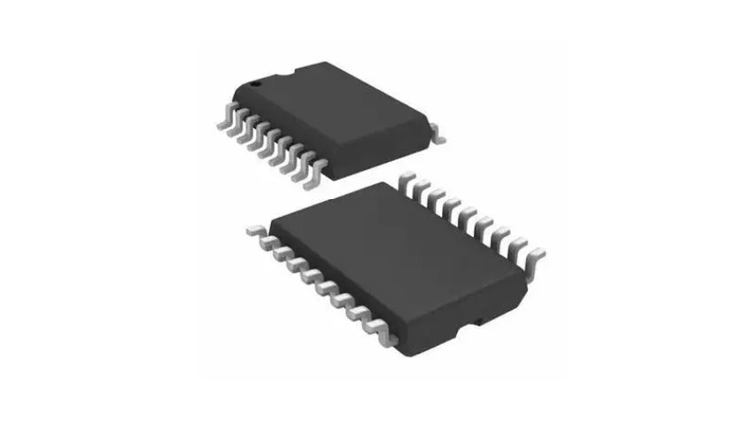
24/28-pin SSOP, 33-pin QFN package.
Operation temperature range: -40°C to +85°C.


You can get your Holtek MCU HT32F52220-HT32F52230 solution by flling out the form below and we will contact you immediately.
Nyquest MCUs Puya MCUs YF Co-packaged MCUs Holtek MCUs Customized PCBA Design
Company Profile Certificates Terms & Conditions Privacy Statement


 MCU Solutions
 PCBA Solutions
 FAQ
FAQ Contact Us
 Company News
 MCU News
 PCBA News
 Company Profile
 Certificates
 Terms & Conditions
 Privacy Statement